Microscope
Background Information
SOS Children have produced a selection of wikipedia articles for schools since 2005. SOS Children is the world's largest charity giving orphaned and abandoned children the chance of family life.
 |
|
| Uses | Small sample observation |
|---|---|
|
Notable experiments
|
Discovery of cells |
| Inventor | Zacharias Janssen |
| Related items | Optical microscope Electron microscope |
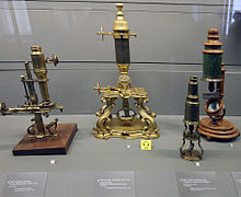
A microscope (from the Ancient Greek: μικρός, mikrós, "small" and σκοπεῖν, skopeîn, "to look" or "see") is an instrument used to see objects that are too small for the naked eye. The science of investigating small objects using such an instrument is called microscopy. Microscopic means invisible to the eye unless aided by a microscope.
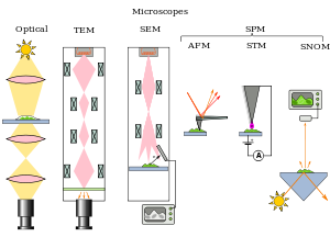
There are many types of microscopes, the most common and first to be invented is the optical microscope which uses light to image the sample. Other major types of microscopes are the electron microscope (both the transmission electron microscope and the scanning electron microscope) and the various types of scanning probe microscope.
History
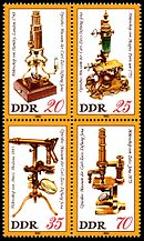
The first microscope to be developed was the optical microscope, although the original inventor is not easy to identify. An early microscope was made in 1590 in Middelburg, Netherlands. Two eyeglass makers are variously given credit: Hans Lippershey (who developed an early telescope) and Zacharias Janssen. Giovanni Faber coined the name microscope for Galileo Galilei's compound microscope in 1625 (Galileo had called it the "occhiolino" or "little eye").
Rise of modern light microscopy
The first detailed account of the interior construction of living tissue based on the use of a microscope did not appear until 1644, in Giambattista Odierna's L'occhio della mosca, or The Fly's Eye.
It was not until the 1660s and 1670s that the microscope was used extensively for research in Italy, The Netherlands and England. Marcelo Malpighi in Italy began the analysis of biological structures beginning with the lungs. Robert Hooke's Micrographia had a huge impact, largely because of its impressive illustrations. The greatest contribution came from Antonie van Leeuwenhoek who discovered red blood cells and spermatozoa and helped popularise microscopy as a technique. On 9 October 1676, Van Leeuwenhoek reported the discovery of micro-organisms.
In 1893 August Köhler developed a key technique for sample illumination, Köhler illumination, which is central to modern light microscopy. This method of sample illumination gives rise to extremely even lighting and overcomes many limitations of older techniques of sample illumination. Further developments in sample illumination came from Fritz Zernike in 1953 and George Nomarski 1955 for their development of phase contrast and differential interference contrast illumination which allow imaging of transparent samples.
Electron microscopy
In the early 1900s a significant alternative to light microscopy was developed, using electrons rather than light to generate the image. Ernst Ruska started development of the first electron microscope in 1931 which was the transmission electron microscope (TEM). The transmission electron microscope works on the same principle as an optical microscope but uses electrons in the place of light and electromagnets in the place of glass lenses. Use of electrons instead of light allows a much higher resolution.
Development of the transmission electron microscope was quickly followed in 1935 by the development of the scanning electron microscope by Max Knoll.
Electron microscopes quickly became popular following the Second World War. Ernst Ruska, working at Siemens developed the first commercial transmission electron microscope and major scientific conferences on electron microscopy started being held in the 1950s. In 1965 the first commercial scanning electron microscope was developed by Professor Sir Charles Oatley and his postgraduate student Gary Stewart and marketed by the Cambridge Instrument Company as the "Stereoscan".
Scanning probe microscopy
The 1980s saw the development of the first scanning probe microscopes. The first was the scanning tunneling microscope in 1981, developed by Gerd Binnig and Heinrich Rohrer. This was closely followed in 1986 with Gerd Binnig, Quate, and Gerber's invention of the atomic force microscope.
Fluorescence and light microscopy
The most recent developments in light microscope largely centre on the rise of fluorescence microscopy in biology. During the last decades of the 20th century, particularly in the post- genomic era, many techniques for fluorescent labeling of cellular structures were developed. The main groups of techniques are small chemical staining of cellular structures, for example DAPI to label DNA, use of antibodies conjugated to fluorescent reporters, see immunofluorescence, and fluorescent proteins, such as green fluorescent protein. These techniques use these different fluorophores for analysis of cell structure at a molecular level in both live and fixed samples.
The rise of fluorescence microscopy drove the development of a major modern microscope design, the confocal microscope. The principle was patented in 1957 by Marvin Minsky, although laser technology limited practical application of the technique. It was not until 1978 when Thomas and Christoph Cremer developed the first practical confocal laser scanning microscope and the technique rapidly gained popularity through the 1980s.
Much current research (in the early 21st century) on optical microscope techniques is focused on development of superresolution analysis of fluorescently labeled samples. Structured illumination can improve resolution by around two to four times and techniques like stimulated Emission Depletion microscopy are approaching the resolution of electron microscopes.
Types
Microscopes can be separated into several different classes. One grouping is based on what interacts with the sample to generate the image, i.e., light or photons(optical microscopes), electrons (electron microscopes) or a probe (scanning probe microscopes). Alternatively, microscopes can be classed on whether they analyse the sample via a scanning point (confocal optical microscopes, scanning electron microscopes and scanning probe microscopes) or analyse the sample all at once (wide field optical microscope and transmission electron microscopes).
Wide field optical microscopes and transmission electron microscopes use the theory of lenses (optics for light microscopes and electromagnet lenses for electron microscopes) in order to magnify the image generated by the passage of a wave transmitted through the sample, or reflected by the sample. The waves used are electromagnetic (in optical microscopes) or electron beams (in electron microscopes). Resolution in these microscopes is limited by the wavelength of the radiation used to image the sample, where shorter wavelengths allow for a higher resolution.
Scanning optical and electron microscopes, like the confocal microscope and scanning electron microscope, use lenses to focus a spot of light or electrons onto the sample then analyze the reflected or transmitted waves. The point is then scanned over the sample to analyze a rectangular region. Magnification of the image is achieved by displaying the data from scanning a physically small sample area on a relatively large screen. These microscopes have the same resolution limit as wide field optical, probe, and electron microscopes.
Scanning probe microscopes also analyze a single point in the sample and then scan the probe over a rectangular sample region to build up an image. As these microscopes do not use electromagnetic or electron radiation for imaging they are not subject to the same resolution limit as the optical and electron microscopes described above.
Optical
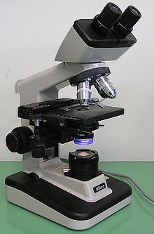
The most common type of microscope (and the first invented) is the optical microscope. This is an optical instrument containing one or more lenses producing an enlarged image of a sample placed in the focal plane. Optical microscopes have refractive glass and occasionally of plastic or quartz, to focus light into the eye or another light detector. Mirror-based optical microscopes operate in the same manner. Typical magnification of a light microscope, assuming visible range light, is up to 1500x with a theoretical resolution limit of around 0.2 micrometres or 200 nanometres. Specialized techniques (e.g., scanning confocal microscopy, Vertico SMI) may exceed this magnification but the resolution is diffraction limited. The use of shorter wavelengths of light, such as the ultraviolet, is one way to improve the spatial resolution of the optical microscope, as are devices such as the near-field scanning optical microscope.
Sarfus, a recent optical technique increases the sensitivity of standard optical microscope to a point it becomes possible to directly visualize nanometric films (down to 0.3 nanometre) and isolated nano-objects (down to 2 nm-diameter). The technique is based on the use of non-reflecting substrates for cross-polarized reflected light microscopy.
Ultraviolet light enables the resolution of microscopic features, as well as to image samples that are transparent to the eye. Near infrared light can be used to visualize circuitry embedded in bonded silicon devices, since silicon is transparent in this region of wavelengths.
In fluorescence microscopy, many wavelengths of light, ranging from the ultraviolet to the visible can be used to cause samples to fluoresce to allow viewing by eye or with the use of specifically sensitive cameras.
Phase contrast microscopy is an optical microscopy illumination technique in which small phase shifts in the light passing through a transparent specimen are converted into amplitude or contrast changes in the image. The use of phase contrast does not require staining to view the slide. This microscope technique made it possible to study the cell cycle in live cells.
The traditional optical microscope has more recently evolved into the digital microscope. In addition to, or instead of, directly viewing the object through the eyepieces, a type of sensor similar to those used in a digital camera is used to obtain an image, which is then displayed on a computer monitor. These sensors may use CMOS or charge-coupled device (CCD) technology, depending on the application.
Electron
Three major variants of electron microscopes exist:
- Scanning electron microscope ( SEM): looks at the surface of bulk objects by scanning the surface with a fine electron beam. See also environmental scanning electron microscope (ESEM).
- Transmission electron microscope ( TEM): passes electrons through the sample, analogous to basic optical microscopy. This requires careful sample preparation, since electrons are scattered so strongly by most materials.This is a scientific device that allows people to see objects that could normally not be seen by the naked or unaided eye.
Scanning probe
- AFM, atomic force microscopy
- BEEM, ballistic electron emission microscopy
- EFM, electrostatic force microscope
- ESTM electrochemical scanning tunneling microscope
- FMM, force modulation microscopy
- KPFM, kelvin probe force microscopy
- MFM, magnetic force microscopy
- MRFM, magnetic resonance force microscopy
- NSOM, near-field scanning optical microscopy (or SNOM, scanning near-field optical microscopy)
- PFM, piezo force microscopy
- PSTM, photon scanning tunneling microscopy
- PTMS, photothermal microspectroscopy/microscopy
- SAP, scanning atom probe
- SCM, scanning capacitance microscopy
- SECM, scanning electrochemical microscopy
- SGM, scanning gate microscopy
- SICM, scanning ion-conductance microscopy
- SPSM spin polarized scanning tunneling microscopy
- SThM, scanning thermal microscopy
- STM, scanning tunneling microscopy
- SVM, scanning voltage microscopy
- SHPM, scanning Hall probe microscopy
- SSM, Scanning SQUID microscope
Of these techniques AFM and STM are the most commonly used.
Other types
Scanning acoustic microscopes use sound waves to measure variations in acoustic impedance. Similar to Sonar in principle, they are used for such jobs as detecting defects in the subsurfaces of materials including those found in integrated circuits.

