Electrical Conduction in Solids
There are two general categories of semiconductors: intrinsic semiconductors, which are composed of only one material, and extrinsic semiconductors, which have had other substances added to them to alter their properties. In semiconductor production, the process of creating extrinsic semiconductors by adding substances to a pure semiconductor for the purposes of modulating its electrical properties is known as doping. Semiconductors are doped to generate either a surplus or a deficiency in valence electrons.
Energy Bands in Solids
Electrons in free atoms have discrete energy values. In contrast, the energy states available to the free electrons in a metal sample form a continuum of "energy bands." In the atomic lattice of a substance, there is a set of filled atomic energy "bands" with a full complement of electrons, and a set of higher energy unfilled "bands" which have no electrons. The highest energy band contains valence electrons available for chemical reactions. The conduction band is the band above the valence band. Electrons in the conduction band are free to move about in the lattice and can conduct current. In order for a substance to conduct electricity, its valence electrons must cross the band gap, which is the energy gap between the valence band and conduction band.
Band Structure
The gap between the valence and conduction bands determines whether a substance will conduct electricity.
If the gap between the valence and conduction bands is large, then the substance does not conduct electricity easily (it is an insulator). On the other hand, these bands overlap in metallic samples, which make these samples excellent conductors of electricity. In the case of semiconductors, the gap is small enough for electrons to jump to the conduction band due to thermal or some other excitation.
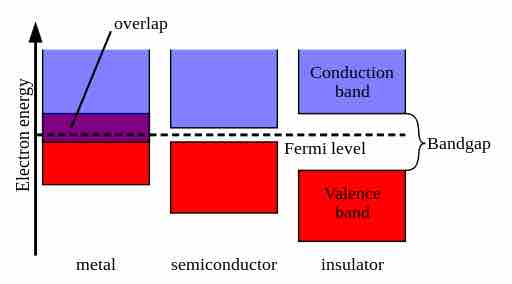
Energy Bands in Solids
The overlap or size of the gap between the valence and conduction bands determines the electrical conductivity of a substance.
Because the band gap is so small for semiconductors, doping with small amounts of impurities can dramatically increase the conductivity of the material. Doping, therefore, allows scientists to exploit the properties of sets of elements referred to as "dopants" in order to modulate the conductivity of a semiconductor.
Semiconductor Doping
There are two types of dopants, n-type ("n" for negative), and p-type ("p" for positive) dopants. n-type dopants act as electron donors and have extra valence electrons with energies very close to the conduction band. When incorporated into the atomic lattice of a semiconductor, the valence electrons of n-type dopants can be easily excited to the conduction band. p-type dopants assist in conduction by accepting electrons. When a p-type dopant is incorporated into the atomic lattice of a semiconductor, it is able to host electrons from the conduction band, allowing the easy formation of positive holes.
Generating an n-Type Semiconductor
When doping a semiconductor, such as the group IV element silicon (Si), with arsenic (As), a pentavalent n-type dopant from group V in the periodic table (which has one more valence electron than the semiconductor), the dopant behaves as an electron donor. When this occurs, an atom of dopant replaces an atom of silicon in the lattice, and therefore an extra valence electron is introduced into the structure. The fifth valence electron of As creates a surplus of electrons. When just a few atoms of the dopant replace silicon atoms in the lattice, an n-type semiconductor is created. The newly created semiconductor is better able to conduct current than the pure semiconductor.
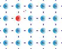
Doping a Silicon Crystal with the n-Type Dopant Arsenic
Doping a pure silicon semiconductor with the group V dopant arsenic creates a surplus of conductive electrons.
Generating a p-Type Semiconductor
When a group IV semiconductor is doped with a p-type trivalent group III dopant (such as boron, B), which has one less valence electron than the semiconductor, the dopant acts as an electron acceptor. When a few atoms of trivalent dopant replace silicon atoms in the lattice, a vacant state (or electron "hole") is created and can act as electron carrier through the structure, which creates a p-type semiconductor. p-type semiconductors are characterized by a deficit of electrons and positive holes, which have the same effect as a surplus of positive charge. These positive holes accept electrons, rendering the semiconductor more effective at conducting current.
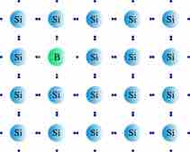
Doping a Silicon Crystal with the p-Type Dopant Boron
Doping a pure silicon semiconductor with the group III dopant boron results in a deficit of conductive electrons and creates a positive hole.
The p-n Junction
When we place p-type and n-type semiconductors in contact with one another, a p-n junction is formed. p-n junctions are basic components of most common electrical devices. While semiconductors doped with either n-type dopants or p-type dopants are better conductors than intrinsic semiconductors, interesting properties emerge when p- and n-type semiconductors are combined to form a p-n junction.
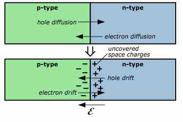
P-n junction diffusion and drift
Diagram of the diffusion across a p-n junction, with the resultant uncovered space charges, the electric field and the drift currents.
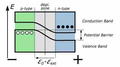
Reverse-biased p-n junction bands
Diagram of a p-n junction under reverse bias, showing conduction and valence bands, the depletion zone, the potential barrier, the resultant electric field,
If no electricity is being passed through the system, then no current passes through the junction between n- and p-type semiconductors. In this scenario, the surplus of electrons from the n-type semiconductor and the deficiency in electrons from the p-type semiconductor combine to create a depletion region. In this state, the system is said to be at equilibrium. However, if the cathode of a battery is connected to the p-type semiconductor, and the anode is connected to the n-type semiconductor, the system is said to be "forward biased." In this scenario, electrons flow from the anode toward the cathode pole and charge flows across the junction. If the connectivity is reversed, with the battery anode connected to the p-type semiconductor and the cathode connected to the n-type semiconductor, the system is said to be "reverse biased" and negligible charge flows across the junction. Combining n-type and p-type semiconductors creates a system which has useful applications in modern electronics.
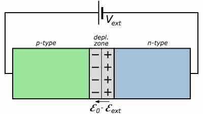
Forward Biased p-n Junction
If the cathode of a battery is connected to the p-type semiconductor while the anode is connected to the n-type semiconductor, the system is said to be forward biased and current flows through the junction.
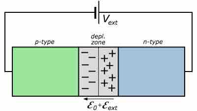
Reverse Biased p-n Junction
If the battery anode is connected to the p-type semiconductor and the cathode connected to the n-type semiconductor, the system is said to be reverse biased and negligible current passes.
Electronic devices and instruments, such as digital alarm clocks, mp3 players, computer processors, and the electronics in cell phones, all take advantage of semiconductor technology. Doping provides a way to modulate the properties of semiconductors that have broad applications in daily life.