Semiconductors are materials that have properties of both normal conductors and insulators. Semiconductors fall into two broad categories:
- Intrinsic semiconductors are composed of only one kind of material; silicon and germanium are two examples. These are also called "undoped semiconductors" or "i-type semiconductors. "
- Extrinsic semiconductors, on the other hand, are intrinsic semiconductors with other substances added to alter their properties -- that is to say, they have been doped with another element.
Intrinsic Semiconductors
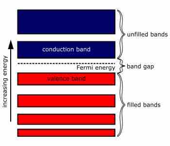
In the classic crystalline semiconductors, electrons can have energies only within certain bands (ranges of energy levels). The energy of these bands is between the energy of the ground state and the free electron energy (the energy required for an electron to escape entirely from the material). The energy bands correspond to a large number of discrete quantum states of the electrons. Most of the states with low energy (closer to the nucleus) are occupied, up to a particular band called the valence band.
Semiconductors and insulators are distinguished from metals by the population of electrons in each band. The valence band in any given metal is nearly filled with electrons under usual conditions. In semiconductors, only a few electrons exist in the conduction band just above the valence band, and an insulator has almost no free electrons.

An Illustration of the Electronic Band Structure of a Semiconductor
This is a comprehensive illustration of the molecular orbitals in a bulk material. As the energy in the system increases, electrons leave the valence band and enter the conduction band.
Semiconductors and insulators are further distinguished by the relative band gap. In semiconductors, the band gap is small, allowing electrons to populate the conduction band. In insulators, it is large, making it difficult for electrons to flow through the conduction band.
Extrinsic Semiconductors
The name "extrinsic semiconductor" can be a bit misleading. While insulating materials may be doped to become semiconductors, intrinsic semiconductors can also be doped, resulting in an extrinsic semiconductor. There are two types of extrinsic semiconductors that result from doping: atoms that have an extra electron (n-type for negative, from group V, such as phosphorus) and atoms that have one fewer electron (p-type for positive, from group III, such as boron).
In semiconductor production, doping intentionally introduces impurities into an extremely pure, or intrinsic, semiconductor for the purpose of changing its electrical properties. The impurities depend on the type of semiconductor. Lightly and moderately doped semiconductors are referred to as extrinsic. When a semiconductor is doped to such a high level that it acts more like a conductor than a semiconductor, it is referred to as degenerate.
N-Type Semiconductors
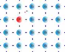
N-type semiconductors are a type of extrinsic semiconductor in which the dopant atoms are capable of providing extra conduction electrons to the host material (e.g. phosphorus in silicon). This creates an excess of negative (n-type) electron charge carriers.

N-type Semiconductor
After the material has been doped with phosphorus, an extra electron is present.
Doping atom usually have one more valence electron than one type of the host atoms. The most common example is atomic substitution in group-IV solids by group-V elements. The situation is more uncertain when the host contains more than one type of atom. For example, in III-V semiconductors such as gallium arsenide, silicon can be a donor when it substitutes for gallium or an acceptor when it replaces arsenic. Some donors have fewer valence electrons than the host, such as alkali metals, which are donors in most solids.
P-Type Semiconductors
A p-type (p for "positive") semiconductor is created by adding a certain type of atom to the semiconductor in order to increase the number of free charge carriers. When the doping material is added, it takes away (accepts) weakly bound outer electrons from the semiconductor atoms. This type of doping agent is also known as an acceptor material, and the vacancy left behind by the electron is known as a hole. The purpose of p-type doping is to create an abundance of holes.

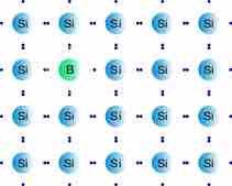
P-type Semiconductor
After the material has been doped with boron, an electron is missing from the structure, leaving a hole. This allows for easier electron flow.
In the case of silicon, a trivalent atom is substituted into the crystal lattice. The result is that one electron is missing from one of the four covalent bonds normally part of the silicon lattice. Therefore the dopant atom can accept an electron from a neighboring atom's covalent bond to complete the fourth bond. This is why these dopants are called acceptors.
When the dopant atom accepts an electron, this causes the loss of half of one bond from the neighboring atom, resulting in the formation of a hole. Each hole is associated with a nearby negatively charged dopant ion, and the semiconductor remains electrically neutral overall. However, once each hole has wandered away into the lattice, one proton in the atom at the hole's location will be "exposed" and no longer cancelled by an electron. This atom will have three electrons and one hole surrounding a particular nucleus with four protons.
For this reason a hole behaves as a positive charge. When a sufficiently large number of acceptor atoms are added, the holes greatly outnumber thermally excited electrons. Thus, holes are the majority carriers, while electrons become minority carriers in p-type materials.